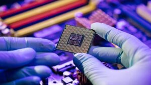
NVIDIA is working with major semiconductor companies to bring artificial intelligence (AI) deeper into chip design, manufacturing, and testing, with reported performance gains of up to 50x in selected inspection workloads. The initiative centres on NVIDIA AI-defined fabs, semiconductor factories that use AI to model processes, identify production problems, and digitally test changes before applying them on factory floors.
Applied Materials, Cadence, KLA, Lam Research, Siemens, Synopsys and other industry players are adopting NVIDIA’s accelerated computing software and AI tools.
The company announced the developments, introducing new tools intended to help engineers accelerate simulations, detect defects and improve manufacturing efficiency.
Also Read: ‘100% Liquid Cooling’: NVIDIA Unveils Technology That Could Nearly Eliminate Data Centre Water Use
NVIDIA cuPotential Targets Faster Chip Design Simulations
NVIDIA introduced cuPotential, a new CUDA-X library developers can use to build AI agents that simulate interactions between atoms and molecules. Such calculations help researchers understand semiconductor materials but can be time-consuming.
NVIDIA said early-access testing showed cuPotential accelerated existing GPU-optimised workflows by an additional two to three times. Synopsys is among its early adopters.
Other reported results include a potential 30-fold speed-up in Synopsys’ QuantumATK simulations using cuEST and a 12-fold improvement in S-Device benchmarks using cuDSS. Cadence reported that its AuraStack AI Super Agent could optimise advanced packaging for heat and stress eight times faster using cuDSS with Celsius.
COMSOL reported simulations up to 10 times faster, while Voltai said its Voltaire platform could reduce complex three-dimensional chip simulation workflows from months to a day.
Also Read: NVIDIA to Buy Hugging Face for $12.9 Billion in Major Open-Source AI Bet
Chip Manufacturing and Inspection Get a Boost
NVIDIA’s open-source NanoVDB library is helping accelerate manufacturing simulations. Lam Research plans to integrate it into SEMulator3D, with selected wafer-etch modelling expected to become up to 30 times faster. NVIDIA PhysicsNeMo has also demonstrated plasma-prediction simulations taking milliseconds instead of days.
In inspection, KLA reported that a new image-processing kernel was 50 times faster than earlier CPU versions. Teradyne reported probe-maintenance inference that was about 85 times faster, helping identify degrading equipment before it affects production yield.
Meanwhile, Imec reported a 30% improvement in the lithography process window using NVIDIA technologies. Advantest is applying AI to production analytics and semiconductor testing, while Siemens is using cuLitho to accelerate chip-pattern refinement.
Also Read: NVIDIA Unveils 24/7 AI Agents for Telecom Networks as Industry Pushes Towards Autonomous Operations
AI-Defined Fabs Expand Into Factory Automation
Applied Materials showed chamber simulations up to 35 times faster & is developing digital factory models to optimise layouts and material movement. FANUC and Foxconn are using NVIDIA Omniverse to test robotic operations in virtual factory environments before physical deployment. OMRON is applying AI agents to inspection analysis and troubleshooting.
NVIDIA cuPotential is available in early access. NanoVDB is open source within OpenVDB, while NVIDIA NPP is available through the CUDA Toolkit. Lam Research’s NanoVDB-accelerated SEMulator3D capability is targeted for release by the end of 2026.
The next measure of progress will be whether these reported gains translate into higher production yields, shorter development cycles and more efficient semiconductor manufacturing at scale.

Samarjit Kaur is a journalist and communications professional covering technology & emerging digital trends. With a focus on clarity and context, she reports on developments shaping industries and governance. When not reporting, she chooses to plug-in and relax on her playlists and plan her next bucket-list trips!