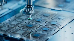
India’s first 3D semiconductor fabrication facility in Odisha has secured full production capacity even before its official launch. The moment reflects rising demand for advanced chip packaging and a growing domestic semiconductor ecosystem.
Industry experts said that early bookings show the confidence of global and domestic clients as India pushes to strengthen its position in the semiconductor value chain.
The facility, expected to focus on advanced 3D chip packaging technologies, is being positioned as a key step in reducing import dependence and supporting sectors such as electronics, telecom and automotive.
Also Read: India Clears First Ever Semiconductor SEZ for Tata’s ₹91,000 Crore Chip Plant at Dholera
Strong Pre-Launch Demand Shows Industry Shift
According to sources familiar with the development, the plant has already committed its initial capacity to multiple clients. This includes companies in high-performance computing, artificial intelligence (AI) and consumer electronics.
The early uptake suggests a shift towards advanced semiconductor solutions that offer better performance and efficiency.
3D semiconductor technology enables chip stacking, improving performance and reducing power consumption. The demand for such solutions has grown globally as companies look to support data-heavy applications, including AI workloads and next-generation devices.
Securing full capacity before launch reduces early-stage risk for the project and it is a strong market aligner. It also reflects growing trust in India’s nascent semiconductor manufacturing capabilities, which remain behind those of global hubs.
Also Read: India’s Semiconductor Mission to Boost R&D Push, MeitY Signals Policy Shift Toward Innovation
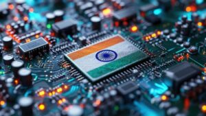
Boost to India’s Semiconductor Ambitions
The Odisha facility comes under the Indian government’s plan to build a domestic semiconductor ecosystem through incentives, policy support and partnerships.
The project aligns with broader efforts to attract investments across chip design, fabrication and packaging. Advanced packaging units like this can play an important role in India’s semiconductor roadmap, as they need lower capital investment than full-scale fabrication plants while still delivering strategic value.
The development is expected to generate employment, strengthen local supply chains and support India’s ambitions to become a global electronics manufacturing hub. With demand already locked in, the plant could serve as a benchmark for future semiconductor projects in the country.

Samarjit Kaur is a journalist and communications professional covering technology & emerging digital trends. With a focus on clarity and context, she reports on developments shaping industries and governance. When not reporting, she chooses to plug-in and relax on her playlists and plan her next bucket-list trips!