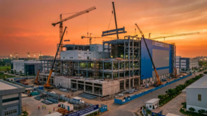
The Indian government is preparing to roll out the second phase of its semiconductor incentive programme with a proposed outlay of ₹1.2 lakh crore. With the plan ready, the government aims to strengthen domestic chip manufacturing and design capabilities.
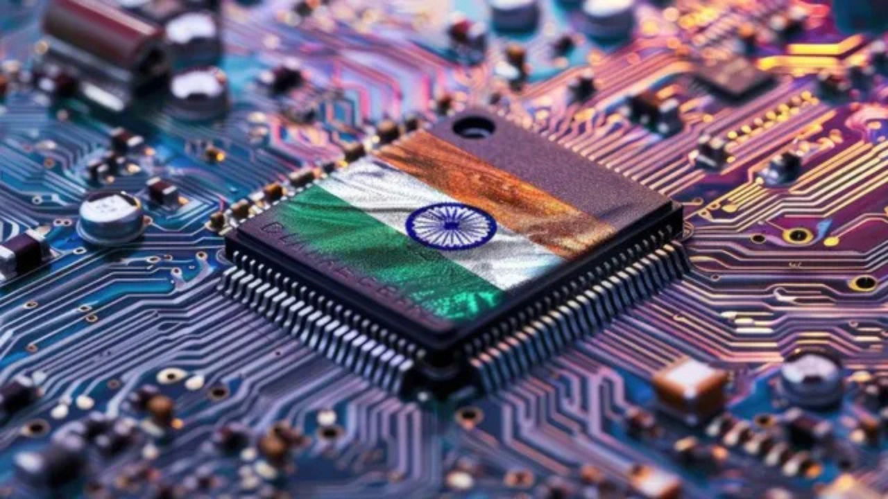
The move comes as part of the strategy to reduce dependence on imports and position India as a global semiconductor hub. Semiconductor Mission 2.0 will be built on the initial scheme while addressing gaps in execution, funding and ecosystem development.
Also Read: Sold Out Before Start: India’s First 3D Semiconductor Plant Sees Full Capacity Lock-In
Focus on Scaling Manufacturing and Design Capabilities
The upcoming Semiconductor Mission 2.0 is expected to prioritise both fabrication and design-led incentives.
The first phase of the programme saw mixed progress, with a few large proposals still under evaluation and execution timelines delayed. The new phase has a refined strategy to streamline approvals and have global players alongside domestic firms.
“The revised framework is likely to include higher fiscal support for advanced chip manufacturing units and compound semiconductor facilities. There is also a renewed focus on supporting chip design startups, which are an important part of the semiconductor value chain.”
-Government officials
India is developing a full-stack semiconductor ecosystem that covers fabrication, assembly, testing, packaging and design. The new phase will align incentives across these segments to create long-term capacity rather than isolated investments.
The Centre is also working to improve coordination with states offering land, infrastructure, and policy support for semiconductor projects. Several states have already announced dedicated semiconductor policies to attract investments.
Also Read: India Clears First Ever Semiconductor SEZ for Tata’s ₹91,000 Crore Chip Plant at Dholera
Addressing Gaps from First Phase, Boosting Global Competitiveness
Officials involved in the planning further said that the second phase will address challenges faced during the initial rollout.
These include:
- Delays in approvals
- Funding disbursement issues
- Clear policy guidelines
The government will soon introduce stricter timelines and improved monitoring mechanisms. The revised mission is also likely to focus on attracting global semiconductor firms amid geopolitical shifts and supply chain diversification.
Countries worldwide are increasing investments in chip manufacturing and India is seeking to secure a share of this global shift. Industry stakeholders have highlighted the need for stable policy support, skilled workforce development and reliable infrastructure, such as power and water supply.
Semiconductor Mission 2.0 is expected to include provisions to address these concerns, as well as incentives for research and development.
The move comes at a time when India is expanding its electronics manufacturing base and pushing for self-reliance in critical technologies. With rising demand for semiconductors across sectors such as automotive, telecom and consumer electronics, the government sees this as a strategic sector for long-term growth.